- 您现在的位置:买卖IC网 > Sheet目录494 > NVMFD5877NLT1G (ON Semiconductor)MOSFET N-CH 60V 17A 8SOIC
�� �
�
�NVMFD5877NL,� NVMFD5877NLWF�
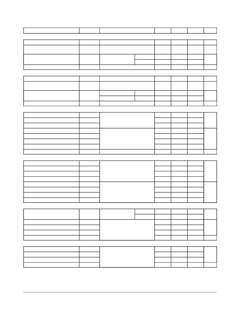
�ELECTRICAL� CHARACTERISTICS� (T� J� =� 25� °� C� unless� otherwise� specified)�
�Parameter�
�Symbol�
�Test� Condition�
�Min�
�Typ�
�Max�
�Unit�
�OFF� CHARACTERISTICS�
�Drain� ?� to� ?� Source� Breakdown� Voltage�
�Drain� ?� to� ?� Source� Breakdown� Voltage�
�Temperature� Coefficient�
�V� (BR)DSS�
�V� (BR)DSS� /T� J�
�V� GS� =� 0� V,� I� D� =� 250� m� A�
�60�
�53�
�V�
�mV/� °� C�
�Zero� Gate� Voltage� Drain� Current�
�I� DSS�
�V� GS� =� 0� V,�
�V� DS� =� 60� V�
�T� J� =� 25� °� C�
�T� J� =� 125� °� C�
�1.0�
�10�
�m� A�
�Gate� ?� to� ?� Source� Leakage� Current�
�I� GSS�
�V� DS� =� 0� V,� V� GS� =� ±� 20� V�
�±� 100�
�nA�
�ON� CHARACTERISTICS� (Note� 5)�
�Gate� Threshold� Voltage�
�Negative� Threshold� Temperature�
�Coefficient�
�V� GS(TH)�
�V� GS(TH)� /T� J�
�V� GS� =� V� DS� ,� I� D� =� 250� m� A�
�1.0�
�3.5�
�3.0�
�V�
�mV/� °� C�
�Drain� ?� to� ?� Source� On� Resistance�
�R� DS(on)�
�V� GS� =� 10� V�
�I� D� =� 7.5� A�
�31�
�39�
�m� W�
�V� GS� =� 4.5� V�
�I� D� =� 7.5� A�
�42�
�60�
�Forward� Transconductance�
�g� FS�
�V� DS� =� 15� V,� I� D� =� 5.0� A�
�7.0�
�S�
�CHARGES� AND� CAPACITANCES�
�Input� Capacitance�
�C� iss�
�540�
�pF�
�Output� Capacitance�
�Reverse� Transfer� Capacitance�
�C� oss�
�C� rss�
�V� GS� =� 0� V,� f� =� 1.0� MHz,� V� DS� =� 25� V�
�55�
�36�
�Total� Gate� Charge�
�Q� G(TOT)�
�5.9�
�nC�
�Threshold� Gate� Charge�
�Gate� ?� to� ?� Source� Charge�
�Gate� ?� to� ?� Drain� Charge�
�Q� G(TH)�
�Q� GS�
�Q� GD�
�V� GS� =� 4.5� V,� V� DS� =� 48� V,�
�I� D� =� 5.0� A�
�0.62�
�1.64�
�2.80�
�Total� Gate� Charge�
�Q� G(TOT)�
�V� GS� =� 10� V,� V� DS� =� 48V,� I� D� =� 5.0A�
�11�
�20�
�nC�
�SWITCHING� CHARACTERISTICS� (Note� 6)�
�Turn� ?� On� Delay� Time�
�t� d(on)�
�8.1�
�ns�
�Rise� Time�
�Turn� ?� Off� Delay� Time�
�Fall� Time�
�t� r�
�t� d(off)�
�t� f�
�V� GS� =� 4.5� V,� V� DS� =� 48� V,�
�I� D� =� 5.0� A,� R� G� =� 2.5� W�
�15.8�
�11.8�
�3.9�
�Turn� ?� On� Delay� Time�
�t� d(on)�
�4.9�
�ns�
�Rise� Time�
�Turn� ?� Off� Delay� Time�
�Fall� Time�
�t� r�
�t� d(off)�
�t� f�
�V� GS� =� 10� V,� V� DS� =� 48� V,�
�I� D� =� 5.0� A,� R� G� =� 2.5� W�
�6.4�
�14.5�
�2.4�
�DRAIN� ?� SOURCE� DIODE� CHARACTERISTICS�
�Forward� Diode� Voltage�
�V� SD�
�V� GS� =� 0� V,�
�I� S� =� 5.0� A�
�T� J� =� 25� °� C�
�T� J� =� 125� °� C�
�0.8�
�0.7�
�1.2�
�V�
�Reverse� Recovery� Time�
�t� RR�
�14.5�
�ns�
�Charge� Time�
�Discharge� Time�
�t� a�
�t� b�
�V� GS� =� 0� V,� d� IS� /d� t� =� 100� A/� m� s,�
�I� S� =� 5.0� A�
�11.5�
�3.1�
�Reverse� Recovery� Charge�
�Q� RR�
�11�
�nC�
�PACKAGE� PARASITIC� VALUES�
�Source� Inductance�
�L� S�
�0.93�
�nH�
�Drain� Inductance�
�Gate� Inductance�
�L� D�
�L� G�
�T� A� =� 25� °� C�
�0.005�
�1.84�
�Gate� Resistance�
�R� G�
�1.5�
�W�
�5.� Pulse� Test:� pulse� width� =� 300� m� s,� duty� cycle� v� 2%.�
�6.� Switching� characteristics� are� independent� of� operating� junction� temperatures.�
�http://onsemi.com�
�2�
�发布紧急采购,3分钟左右您将得到回复。
相关PDF资料
NVMFS4841NT1G
MOSFET N-CH 30V 89A SO-8FL
NVMFS5844NLT1G
MOSFET N-CH 60V 11.2S SO-8FL
NVR1P02T1G
MOSFET N-CH 20V 1A SOT-23-3
NVTFS4823NTAG
MSOFET N-CH 30V 30A 8WDFN
NVTFS4824NTAG
MOSFET N-CH 30V 18.2A 8WDFN
NVTFS5116PLTWG
MOSFET P-CH 60V 14A 8WDFN
NVTFS5811NLTAG
MOSFET N-CH 40V 40A 8WDFN
NVTFS5820NLTAG
MOSFET N-CH 60V 37A 8WDFN
相关代理商/技术参数
NVMFD5877NLT3G
功能描述:MOSFET NFET SO8FL 60V 17A 39MOHM RoHS:否 制造商:STMicroelectronics 晶体管极性:N-Channel 汲极/源极击穿电压:650 V 闸/源击穿电压:25 V 漏极连续电流:130 A 电阻汲极/源极 RDS(导通):0.014 Ohms 配置:Single 最大工作温度: 安装风格:Through Hole 封装 / 箱体:Max247 封装:Tube
NVMFD5877NLWF
制造商:ONSEMI 制造商全称:ON Semiconductor 功能描述:60 V, 39 m, 17 A, Dual Na??Channel, Logic Level, Dual SO8FL
NVMFD5877NLWFT1G
制造商:ONSEMI 制造商全称:ON Semiconductor 功能描述:60 V, 39 m, 17 A, Dual Na??Channel, Logic Level, Dual SO8FL
NVMFD5877NLWFT3G
制造商:ONSEMI 制造商全称:ON Semiconductor 功能描述:60 V, 39 m, 17 A, Dual Na??Channel, Logic Level, Dual SO8FL
NVMFS4841NT1G
功能描述:MOSFET Single N-Channel 30V,89A,7mOhm
RoHS:否 制造商:STMicroelectronics 晶体管极性:N-Channel 汲极/源极击穿电压:650 V 闸/源击穿电压:25 V 漏极连续电流:130 A 电阻汲极/源极 RDS(导通):0.014 Ohms 配置:Single 最大工作温度: 安装风格:Through Hole 封装 / 箱体:Max247 封装:Tube
NVMFS4841NT3G
制造商:ONSEMI 制造商全称:ON Semiconductor 功能描述:Power MOSFET 30V, 7 m, 89A, Single N?Channel SO8FL
NVMFS4841NWFT1G
制造商:ON Semiconductor 功能描述:NFET SO8FL 30V 89A 7MOHM - Tape and Reel 制造商:ON Semiconductor 功能描述:REEL - NFET SO8FL 30V 89A 7MOHM
NVMFS5826NL
制造商:ONSEMI 制造商全称:ON Semiconductor 功能描述:Power MOSFET 60 V, 24 m, 26 A, Single Na??Channel